
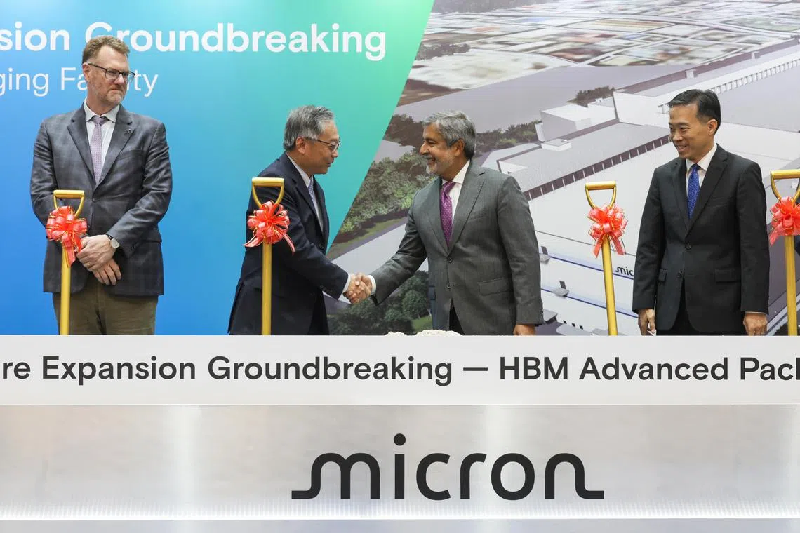
MICRON Technology on Wednesday (Jan 8) broke ground in Woodlands for an advanced packaging facility for its high-bandwidth memory (HBM) semiconductor chip.
The company will invest US$7 billion in the facility adjacent to its existing plant, “through the end of the decade and beyond”, creating around 1,400 jobs. Another 1,600 jobs may be created under plans for future expansions on the site.
HBM chips are used in artificial intelligence (AI) training and inference.
Micron said the new facility will be the first of its kind in Singapore. It will package its latest HBM3E products. Operations are slated to begin in 2026, while “meaningful expansion” of the company’s total advanced packaging capacity will begin in 2027 to meet demand from AI growth.
At the ground-breaking event, Micron president and chief executive officer Sanjay Mehrotra said discussions on the advanced packaging facility had transpired over “several months”.
He added that he was “extremely impressed” by how fast the government worked to bring the project to reality.
BT in your inbox
Start and end each day with the latest news stories and analyses delivered straight to your inbox.
The CEO was also grateful to the company’s academic partners for their contributions to the development of the local semiconductor industry.
He cited a research project between the Agency for Science, Technology and Research (A*Star) and Applied Materials as a “great model of enabling research capabilities”.
“(We’re) really looking forward to taking our partnership with academia to the next level to drive future engines of research and development,” he noted.
At the company’s recent quarterly results for the three months ended last Nov 28, he noted that HBM revenue had doubled sequentially, exceeding expectations.
In his speech on Wednesday, Micron corporate vice-president and Singapore country manager Chen Kok Sing said that since 1998, the company has grown its investments in Singapore to more than US$30 billion. These investments include the establishment of greenfield wafer fabrication sites and the expansion to four wafer fabrication facilities.
He noted that the company’s workforce of more than 9,000 has shifted from pure manufacturing activities to engagement in early-phase research and development.
“Our assembly and test facility in Bendemeer Road, one of Singapore’s longest-running semiconductor facilities for more than half a century, has stayed ahead of the curve as an advanced packaging and test facility for complex, high-value products,” he said.
The event’s guest of honour, Deputy Prime Minister and Minister for Trade and Industry Gan Kim Yong, said Singapore is committed to being a “stable, reliable and trusted partner” for trade and investment.
This is even as geopolitical contestation intensifies and other countries impose export controls and outbound investment screening.
“As the first HBM facility in Singapore, it will allow us to establish a foothold in a new product segment with strong growth potential, especially given the growth of AI,” he said.
He added the government will continue to invest in growing the local semiconductor industry by doubling down on areas of strength, such as speciality semiconductors and Nand memory fabrication. It will also continue to seek out new areas of growth, such as in HBM.
Nand is a form of semiconductor logic gate used in the creation of non-volatile flash memory, such as solid-state drives for storage, which Micron also produces.
“This will, in turn, benefit our larger semiconductor ecosystem, including equipment manufacturers and suppliers, across spares, materials, facilities and services,” he said, adding that this would create more good jobs for Singaporeans.
In response to queries, the Singapore Economic Development Board (EDB) said that in the last two years, the Republic has attracted over S$18 billion in research and development and manufacturing investment commitments into the semiconductor ecosystem.
The EDB tracks these commitments in the form of Fixed Asset Investments (FAI), which mainly refer to incremental capital investment in facilities, equipment and machinery.
FAI commitments are recorded when the company has made a firm undertaking to implement the project or the phase of the project, although the actual transactions may take place in subsequent periods.


